Corel Draw Pcb Design Software
PCB Design Guidelines from our experts in Australia and New Zealand
Hello friends!!
Keep up–to–date with the latest in advanced PCB design technologies.
Let's start by stepping through the basics of PCB design.
- First step is schematic capture or schematic entry is done through an EDA (Electronic Design Automation) tool.
- Card dimensions and template are decided based on required circuitry and case of the PCB. Determine the fixed components and heat sinks if required.
- Deciding stack layers of the PCB. 4 to 12 layers or more depending on design complexity. Ground plane and Power plane are decided. Signal planes, where signals are routed, are in top layer as well as internal layers.
- Line impedance determination using dielectric layer thickness, routing copper thickness and trace-width. Trace separation also taken into account in case of differential signals. Microstrip, stripline or dual stripline can be used to route signals.
- Placement of the components. Thermal considerations and geometry are taken into account. Vias and lands are marked.
- Routing the signal trace. For optimal EMI per formance high frequency signals are routed in internal layers between power or ground planes as power plane behaves as ground for AC.
- And the last step Geber File generation for manufacturing.
DEFINITION
Printed Circuit = Electric circuit in which the conducting paths connecting circuit components are affixed to a flat insulating board.
PWB vs. PCB
- PWB = Printed Wiring Board
Copper traces and pads create point-to-point connection of components. - PCB = Printed Circuit Board
A PWB that contains functional circuits or components that are embedded in the copper.
IN THE BEIGNING
- Engineer
- Concept of design
- Rough "scribble" of schematic
- Breadboard proofing of concept
- Designer
- Hand draw full schematic
- Hand draw layout of component placement (2x, 4x)
- Hand tape circuitry on to mylar film
- Hand inking of components and board nomenclature
- Drill templates created using dots, donuts, symbols
- Manufacturer
- Photo-reduction of taped ar twork
- Chemical etching of copper laminates
- Hand cut silkscreens to squeegee onto board
- "Bulls eye" drilling of holes
- Hand mounting and soldering of components
- Hand probes used to test functionality
ADVANCES MADE
- Manufacturing
- First to utilize advances in automation and computers
- Digitizing replaces photo-reduction
- NC Drill replaced "Bulls eye" drilling
- Photographic imaging to create silkscreens
- "Pick & Place" machines for component mounting
- Wave solder machines reduces hand soldering
- Designing
- Hand drawing layouts digitized to create 1x film ar twork
- CAD programs developed for board layout
- Output of Gerber data to create 1x film ar twork
- Output of NC Drill tapes
TODAY
- Engineer
- Develop concept and schematic in CAD/CAE tools
- Computer simulating design replaces breadboard
- Designer
- CAD tools tie schematic and layout for "Intelligent" Designs
- Component placement and circuit routing automated
- Data output increased to include: Gerber data, NC Drill data, component placement data, net list data, testing data, etc.
- Manufacturer
- Use Gerber and NC Drill data to fabricate bare board
- Use component placement data to assemble board
- Use net list and testing data to verify final product
DESIGN TECHNOLOGY GROWTH
- General population likes what they see and want more
- Industry answers the demands of their Customers
- Technological growth results:
- Smaller product packaging
- More functionality per circuit card
- Smaller components, Sur face Mount and Micro Technology
- Increased component to board area density
- Demand for faster time to market
- Panelization for easier handling
- Increased automation for faster turn around
- Increased Demand for Quality Product
- Statistical Process Control (SPC)
- Used for improving manufacturing and assembly processes
- Statistical Process Control (SPC)
- Concurrent Engineering (CE)
- Design Engineer, PCB Designer, ManufacturingEngineer, Test Engineer, and Quality Engineer all working as a team to develop the ultimate design
- Integrated Product Development System (IPDS)
- Development Team expanded to include the Customer and Suppliers
- Concept to Delivery and Support
- "Design for…" becomes new buzz words for the electronic industry
- DFM, DFT, DFR, DFC…DFX
- Smaller product packaging
INDUSTRY STANDARDS
- Board Level
- IPC-2221 Generic Standard for Printed Board Design
- IPC-4101 Specification for Base Materials
- IPC-4103 Materials for High Speed/High Frequency boards
- IPC-7351 Sur face Mount Design and Land Pattern
- IPC-SM-840 Solder Mask Standard
- IPC-TM-650 Test Methods Manual
- Assembly Level
- IPC-A-610 Acceptability of Printed Board Assemblies
- J-STD-001 Requirements for Soldered Electrical and Electronic Assemblies
- Documentation
- MIL-STD-100 Engineering Drawing Practices
- ASME Y14.100 Replaces MIL-STD-100 for non-Military
- IPC-D-325 Documentation Requirements for Printed Boards, Assemblies and Support Drawings
- ASME Y14.5 Dimensioning and Tolerancing
CLASSES AND TYPES
- 1. Performance Classes
- Determined by End use of product
- 2. Board Types
- Bare board configurations
- 3. Producibility Levels
- Circuit design complexity
- 4. Assembly Classes
- Component mounting complexity
1. PERFORMANCE CLASSES
- Class 1 – General Electronics Products
- Main impor tance is functionality. Cosmetic imper fections not impor tant
- Some computers and computer peripherals
- Class 2 – Dedicated Service Electronics Products
- Extended life and uninterrupted service desired, but not required
- Communications, sophisticated business machines, instruments
- Class 3 – High Reliability Electronics Products
- Continued per formance or per formance on demand is required. Downtime is not acceptable
- Life suppor t systems, critical weapons systems
2. BOARD TYPE
- Type 1 – Single-Sided Printed Board
- Type 2 – Double-Sided Printed Board
- Type 3 – Multilayer without blind and/or buried vias
- Type 4 – Multilayer with blind and/or buried vias
- Type 5 – Multilayer Metal Core without blind and/or buried vias
- Type 6 – Multilayer Metal Core with blind and/or buried vias
3. PRODUCIBILITY LEVELS
- Level A - General Design Complexity
- Preferred
- Level B - Moderate Design Complexity
- Standard
- Level C - High Design Complexity
- Reduced Producibility
4. ASSEMBLY CLASSES
- Class A – Through-hole mounted components only
- Class B – Sur face Mount components only
- Class C – Simplistic through-hole and sur face mount intermixed assembly
- Class X – Complex intermixed assembly (Through-hole, sur face mount, fine pitch and BGA)
- Class Y – Complex intermixed assembly (Through-hole, sur face mount, ultrafine pitch and chip scale)
- Class Z – Complex intermixed assembly (Through-hole, ultrafine pitch, COB, flip-chip and TAB)
COMPONENTS
- Types of Components
- Passive vs. Active
- Symbols and Designations
- Package Types
- Through-hole
- Surface Mount
- Surface Mount Lead Styles
- Polarity and Orientation
TYPES OF COMPONENTS
Passive Components: Basic function does not change when they receive a signals
Active Components: Basic function of component changes when a signal is received
PACKAGES TYPE
Surface Mount - Components with leads that are mounted directly onto lands that are on the surface of the board
| Package Type | Description | Typical Components |
| Chip | Usually ceramic bodied package with metal termination on each and rectangular | Resistors, Capacitors, Inductors, some Diodes |
| MELF | Metal Electrode Face Metal terminations on each end of cylindrical body | Diodes, Resistors |
| LCC | Leadless Chip Carrier No leads, metalization in form of castellations for attachment | ICs |
| SOIC | Small Outline Integrated Circuit Similar to DIP package with leads formed for sur face mounting | ICs |
| QFP | Quad Flat Pack Leads extend from four sides of the component | ICs |
| BGA | Ball Grid Array Sur face mount version of PGA. Leads are tiny metal balls on bottom of component | ICs |
SURFACE MOUNT LEAD TYPE
- Gull Wing - Bends down and away from component
- J-Lead - Bends down and under component
- L-Lead - Inward formed under component
- Flat Lead - Extends straight out from component
- Ball - Tiny metal ball mounted to bottom sur face
- Lead Pitch - Distance from center of one pin to center of adjacent pin
- Standard: 25 - 50 mils
- Fine: 11.8 - 19.7 mils
- Ultrafine: < 11.8 mils
POLARITY AND ORIENTATION
- Polarity
- Positive and negative ends of a two pin device
- Positive or anode lead graphical representation
- Capacitor - Identified with a (+) and/or square pad
- Diode - Identified flat end of triangle and/or square pad
- Negative or cathode lead graphical representation
- Capacitor - Not identified
- Diode - Identified by bar end of diode symbol
- Orientation
- Identification of pin 1 of multi-pin devices
- Dot, notch or number identification on component
- Square pad or silkscreened dot on board sur face
- Pin count direction typically counter-clockwise from pin 1
DOCUMENTATION
Master Drawing
- Supplies all the information needed to fabricate the bare board
- Minimum information required per IPC-D-325:
- Design requirements Silkscreen requirements
- Board detail & construction Marking requirements
- Conductor definition Bow & twist requirements
- Minimum spacing requirements Test coupons requirements
- Artwork configuration control Electrical Test requirements
- Fabrication allowances Per formance requirements
- Solder mask requirements Master pattern drawing
- Reference to CAD data
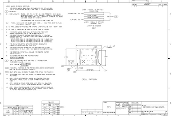
- MASTER DRAWING SAMPLE
Printed Board Assembly Drawing
- PRINTED BOARD ASSEMBLY DRAWING SAMPLE

Parts List – Bill of Materials (BOM)
- Tabulation of all parts and materials used in the construction of a printed board assembly
- Can be a Separate Parts List or Integral Parts List
- Minimum information required per IPC-D-325:
- Item (Find) Number
- Electrical component cross-reference
- part Information
- (1) Components (2) Hardware (3) Bulk Materials
- Quantities
- Referenced Processes
- PART LIST BILL OF MATERIALS(BOM) SAMPLE
| Parts List, 15000173, Revision B2, 7-JAN-97 | ||||||||
| Item | Supplier | Part# | Description | Reference Designator | Assembly Variation Quantity | |||
| 01 | 02 | 03 | 04 | |||||
| 01 | Hadco | 5101342 | Board | BRD1 | 01 | 01 | ||
| 02 | Nec | 8201342 | Board | BRD1 | 01 | 01 | ||
| 03 | Motorola | 1N6378 | Diode | D1, D2 | 02 | 02 | ||
| 04 | Motorola | 1N6337 | Diode | D1, D2 | 02 | 02 | ||
| 05 | HP | 5082-2835 | Diode Schottky | D3 | 01 | 01 | 01 | 01 |
| 06 | Dialight | 550-3007 | Connector, VME 100 pin | J1 | 01 | 01 | 01 | 01 |
| 07 | Signetic | 74HTC126E | IC, Dip | E1 | 01 | 01 | 01 | 01 |
| SUB | Harris | CD74HTC125E | IC, Dip | E1 | 01 | 01 | 01 | 01 |
| 08 | Signetic | 74HTC126E | IC, Dip | E2 | 01 | 01 | ||
| 09 | Harris | CD74HTC125N | IC, Dip | E2 | 01 | 01 | ||
| 10 | Kemet | C322C104M5U5CA | Capacitor, .1uF, 50V, Mono | C1-C3 | 03 | 03 | 03 | 03 |
| 11 | Maxim | MAX238CWG | IC, SMT GULL | E3 | 01 | 01 | 01 | 01 |
| 12 | Kemet | C12062C104K5RAC | Capacitor, 1206 .1uF | C4, C5 | 02 | 02 | 02 | 02 |
| SUB | MEPCO | 12062R104K9BB0 | Capacitor, 1206 .1uF | C4, C5 | 02 | 02 | 02 | 02 |
| 13 | BRADY | LTA-1-652-10 | Label, 0.25 x 1.875 | 01 | 01 | 01 | 01 | |
| 14 | BRADY | LTA-1-655-08 | Label | 01 | 01 | 01 | 01 | |
Schematic Diagram
- Graphical representation of symbols, electrical connections, components and functions of a specific circuit arrangement.
- Minimum information required per IPC-D-325:
- Functional flow left to right, top to bottom
- Reference Designations for each component depicted
- Unused pins
- Spares
- Ground and Power Table
- Highest reference designation used
- Reference designations not used
- Definition of non-standard symbols used
- SCHEMATIC DIAGRAM SAMPLE:

PCB DESIGN PROCESS
This was the basic introduction now we will see PCB design process in detail, which will help you to understand design process very precisely and thoroughly.
- PCB designing process sequence:
- Before the design
- Preparing the design
- Draw the board
- Import the net
- Place the parts
- Route the traces
- Final work
- Post processing
BEFORE THE DESIGN
- You will need (as a minimum)
- The required dimensions of the board
- A list of parts to be used on the board
- The data sheets for each part
- A schematic diagram of the board
- Board Domension
- Where does the board go?
- Into a case
- Slides into a rack
- What are the external dimensions for the board?
- Board requires connections to:
- Obtain power
- Exchange information
- Display results
- Where do the connectors go?
- What size connectors are to be used?
- How is the board held in place?
- Guide rails
- Mounting bracket(s)
- Bolts
- Are there any height restrictions?
- Some components have higher profiles
- Transformers
- Large capacitors
- Batteries
- What thickness of copper should be used?
- The more current to be carried, the thicker the copper has to be.
- Copper laminate thickness is usually given in ounces per square foot
- For general use boards, a common thickness is 1 oz copper (1.4 mil, 0.0014in, 0.035mm, 35m)
- Where does the board go?
- Part List
- Known also as the BOM (bill of materials)
- Each part is must be identified by a unique reference designator and a part description
- e.g. R5 "1 k, ¼ watt metal film resistor, 5%"
- Data Sheet For Each Part
- The most impor tant information is the physical dimensions of the part
- if you do not have a data sheet obtain part and measure it yourself
- not as accurate as using part manufacturer's information, but better than guessing
- The most impor tant information is the physical dimensions of the part
- Schematic Diagram Of The Design
- Shows the connection of the parts on the board
- Each part on schematic has a reference designator that matches that on the BOM
- Most ECAD programs give an automatic generation of the BOM
PREPARING THE DESIGN
Two steps involved here are:
A. Generation of the netlist
B. Creating the parts Database
- Generation of The Netlist
- The netlist is a file that has the device names of the parts used on the board
- It also shows the "nets" - interconnections between the pins of the parts
- Although can be typed by hand if schematic was manually drawn best to let system generate it from the schematic
- The netlist file is critical to PCB function. Should be double checked as the smallest mistake can cause board to be scrapped
- Creating The Parts Database
- Most ECAD systems define the parts to be placed on the board as a special type of file called the PDB file
- Allows better use of computer memory and disk resources by allowing multiple instances
- PDB is built in a hierarchy
- Devices > Packages > Pads
- Pads
- Entities that inter face the part pins to the copper traces of the board
- Pad must be big enough top allow enough copper around a hole (for thru-hole components)
- If pad is too large may have trouble soldering
- Many ECAD systems include solder mask information with the pad files
- Packages
- Entities that represent the part. Consist of lines and text
- Lines represent the maximum dimensions of the part on the assembly drawing and the layout
- Creating The Parts Database
- Lines are also drawn on a different layer to represent the part outline on the silkscreen legend Text shows the designator for the part when placed on the board
- Devices
- Entities that link the value or part number of a part with the ECAD package
- Thus can design one "DIP14" package and a number of device files to link "74S00" and other part numbers to it in the netlist
- On many systems these are text files to allow for selective swapping of pins and mapping of pin numbers to a different pin when inser ted
DRAW THE BOARD
- First draw outline of the board
- Need a datum
- Place tool holes at three corners
- Two are on same ver tical axis and third on same horizontal axis as the first
- Hole at intersection of horizontal and ver tical axis is the datum or (0,0) coordinate of the PCB
- May need to set-up placement keep-out areas:
- if board fits into a card rack need to allow for amount of board that sits in the slides
- a keep-out of 0.050" around board edge to allow for manufacturing tolerances
- May need special keep-out areas:
- to impose height limitations
- to limit what parts and signals may be routed within them
- to allow for testing and assembly
IMPORT THE NETLIST
- The netlist is then read in and associated with any pre-existing fixed parts on the board
- Any errors made will usually be apparent here - automatic error detection is one of the big advantages of using ECAD systems
PLACE THE PARTS
- Placement factors
- Electrical function
- Physical size
- Temperature factors
- Routability
- Most ECAD programs have autoplacement options. Often only good for boards with just a few parts
- Even for manual placement programs have aids
- Ratsnest display shows all connections
- Placement Guidelines
- Can save space by using both sides of the board in the old days parts went on one side called the component side. With the advent of sur face mount this is now the "primary" side, as components can be placed on both sides
- Sur face mount devices are smaller than conventional ones
- Use a standard grid. A common size is 0.025"
- easier to align components
- Place parts in only one or two orientations, ver tical and horizontal
- non-or thogonal angles are harder to assemble
- Place polarized parts in the same orientation to keep assembly and repair errors to a minimum
- all diode cathodes to be up or to the right
- Place IC packages in an even matrix and make sure they are functionally grouped
- power and ground connections will be easier
- Arrange parts so:
- they are evenly spaced
- do not overlap
- their pads are a sufficient distance apart to allow traces to pass between them
- pads should have minimum 0.020" gap in a general purpose board
- Axial parts such as resistors and capacitors should be placed so:
- there is an equal amount of lead wire on either side of the body
- the two pads are at a similar distance as other axial parts
- general value is 0.500" for smaller parts
- Usually should not allow a lead to bend more than twice the lead diameter from the body of the part
- Allow sufficient diameter around mounting holes for hardware to be inser ted and tightened without affecting neighbouring parts
- Allow sufficient distance between parts so that their leads will not touch when bent over to secure them before soldering

- Edge connector device placed to reduce routing length
- Analog circuit placed near output connector to reduce digital noise

- Device driving analog circuit placed adjacent to analog circuit
- Other devices placed according to circuit flow


ROUTING THE BOARD
- Routing is the connecting of the parts that have been placed on the board
- Can be done manually or automatically
- usually better to do automatically
- Even if adopt automatic routing it is good practice to lay out power and ground traces
- use a "rail" structure where possible with parallel ground and power traces between rows of Ics
- use a wide trace for these runs 0.05" for power and 0.100" for ground can usually use 0.025" traces for connecting each part to to the rail but do calculations first
- Good routing strategy normally has traces on side of the board ver tical, with the other horizontal.
- It is cheaper to have signal traces 0.013" on a 0.025" centers. Many shops can do 0.004" on 0.008" centers (or even finer), but this is often overkill
- Good routing strategy normally means trace should be as shor t and direct as possible
- Could be possible to have all signal traces star ting and ending on a component pad
- trace would then snake around so much that circuit function is degraded
- avoid this problem by using pads without component leads. These are called feed-thrus or vias
- Vias allow better routing of the board as ver tical/horizontal strategy is maintained as well as minimizing signal path
- Although professional designers take pride in minimizing number of vias, they lead to better designs
- Critical signals are best done by hand. This allows the signal trace to have less bends and vias than the auto router would use
- Flag the trace before turning on the auto router so that it is not moved
- On a complex board some signals will not be routed and must be finished manually
- This is where the skill of the designer comes in
- If 95% of the board is finished by the auto router, it can be quite time consuming and tricky to finish the last 5% manually
FINAL WORK
- After placement and routing is complete will need to:
- (A) Adjust the silkscreen legend
- (B) Prepare a fabrication drawing
- (C) Prepare an assembly drawing
(A) Adjust The Silkscreen Legend
- part outlines need to be trimmed to keep lines off pads and vias
- many ECAD programs do this automatically
- Reference designators need to be moved for same reason and also so they can be seen when part is installed
- May need other details to be shown
(B) Prepare a fabrication drawing
- Dimensions of board are to be shown in reference to the datum tool hole
- Different symbol should be shown for each hole size
- Table to be given showing quantity of each hole size
(C) Prepare an assembly drawing
- Used as an aid for building and repairing the board
- Outlines of parts and reference designators to be shown
- Any special assembly instructions to be shown
- For simple boards some companies just use a copy of the silkscreen legend as their assembly drawing
POST PROCESSING
- Prepares data that is used by the manufacturer to generate the finished board
- First step is to print the fabrication and assembly drawings
- Should check these before sending out. Correction of mistakes once board has been made are very expensive
- Second step is to generate the NC drill file of hole positions
- Manufacturer uses this data to set-up for drilling the boards
- Can set up drills by optically inputting data from assembly drawing
- this is more expensive and error prone
- better to generate the drill file
- Third step is to generate the ar t work for the board
- Each layer of the board must have a master ar twork with opaque features on a clear background
- May be possible to do printing yourself but better to send to a reprographic company
- Many manufacturers accept photo plot files (gerber files)
PCB DESIGN TOOLS & SOFTWARES
Here is the list of various designing tools and softwares with their applications, which helps you to design your PCB as per your requirement.
- EAGLENice, easy to use CAD/CAM software for PCB schematic and routing. .BRD files for prototyping. You can download free evaluation version.
- gEDAgEDA is a free, open-source schematic capture and layout package that runs on Linux.
- ZenitPCBZenitPCB is a freeware layout software.
- PCBFree unix PCB editor.
- FREE-PCBFreePCB is a free, open-source printed circuit board layout editor for Microsoft Windows!
- TinyCADTinyCAD is a free open-source schematic editor.
- KICADGPL open source schematic capture and PCB routing.
- TCI3Free PCB routing and schematic capture software.
- SCOREFree schematic capture software (Alfa version).
- OSMOND PPCFREE MAC PCB CAD/CAM software.
- MINIMAL PCB EDITOROpen source schematic capture and board layout editor for windows.
- PROTELCAD/CAM software for schematic and routing. You can download 30 days free trial. Protel offers free old-DOS based software called EasyTrax.
- CADSTARCAD/CAM software for schematic and routing. Have free for download limited demo version.
- ORCADCAD/CAM software. No demo/evaluation version.
- CIRCUIT MAKERCAD/CAM software for schematic and routing. You can download limited demo version.
- P-CAD 2000PCB CAD/CAM software. You can download FREE trial version.
- PCB ELEGANCENice looking CAD/CAM software for schematic and routing. You can download limited demo version.
- EDWINCAD/CAM software for schematic and routing. You can download limited demo version.
- VISUALPCYou can download limited demo version.
- BPECS32Very limited PCB CAD software. You can download limited demo version.
- AUTOENGINEERPCB CAD/CAM software. You can download limited demo version.
- EXPERT PCBPCB CAD/CAM software. You can download limited demo version.
- CIRCADPCB CAD/CAM software. You can download limited demo version.
- LAYOUTPCB CAD/CAM software. You can download free version.
- CIRCUIT LAYOUTPCB CAD/CAM software. You can download limited demo version.
- MCCADPCB CAD/CAM software. You can download limited demo version.
- DREAM CADJapanese PCB CAD/CAM software. You can download limited demo version.
- E-CADSupermax CAD/CAM software, runs on NT. You can download limited demo version.
- POWERPCBCAD/CAM software. No demo/evaluation version.
- PCB ASSISTANTLow cost PCB CAD software. You can download limited demo version.
- PCB DESIGNERLow cost PCB CAD software. You can download limited demo version.
- QCADPCB CAD/CAM software. You can download limited demo version.
- QUICK ROUTEPCB CAD/CAM software. You can download limited demo version.
- TARGET 3001PCB CAD/CAM software. You can download limited demo version.
- WIN CIRCUIT 98PCB CAD/CAM software. You can download limited demo version.
- BOARD EDITORLow cost PCB CAD software. You can download free demo version.
- VUTRAXPCB CAD/CAM software. You can download limited demo version.
- CIRCUIT CREATORPCB CAD/CAM software. You can download free demo version.
- PADSPCBPADS PCB CAD/CAM software. You can download free limited demo version on this ftp server.
- DESIGN WORKSPCB schematic capture and simulation software. You can download free evaluation version.
- LAY01PCB CAD/CAM software with limited demo version (200 pins) for free download.
- GElectronicLow cost PCB routing and schematic capture software.
- PRO-Board, PRO-NetSchematic capture and routing for AMIGA computers.
- CSIEDASchematic capture and routing for PC.
- VISUALPCBLow cost schematic capture, spice and routing for PC.
- WINBOARDCAD/CAM software for schematic and routing. You can download limited demo version.
- ULTIBOARDCAD/CAM software for schematic and routing. You can download limited demo version.
- EASY PCPCB CAD/CAM software.
- RANGERPCB CAD/CAM software. You can download limited demo version.
- PROTEUSLow cost CAD/CAM software. You can download limited demo version.
- EPD - Electronics Packaging DesignerRF/hybrid/flex design tools based on AutoCAD.No demo available for direct download.
- AutoTrax EdaSchematic design and PCB routing software. You can download free copy from the web site.
- SprintLayoutLow cost tool to create layouts for single-sided and double-sided PCBs . You can download limited demo version from the web site. NO DRC check which make this program quite useless.
- CADINTSchematic capture and PCB routing. Have 30 days trial version for download.
- Merlin PCB DesignerShareware for Corel Draw which allow PCBs to be routed.
- WINQCADSchematic capture, PCB routing, autorute. Have free 200 pin version for download.
- PulsonixPCB schematic capture and routing software. 100 pin restricted demo available.
- DIPTRACEPCB schematic capture and routing software. 30 days evaluation version. Not-for-profit version available allows 4 layers and 1000 pins.
- RIMU PCBLow cost PCB schematic capture and routing software. Demo version is available for download
- TopoRSchematic capture and PCB layout with some unique features as round edges auto-routing, made in Russia. Demo version is available for download
- TINASchematic capture and PCB layout with analysis and spice. Demo version is available for download.
Corel Draw Pcb Design Software
Source: http://www.qualiecocircuits.com.au/pcb-design-guidelines.html
0 Response to "Corel Draw Pcb Design Software"
Post a Comment